- 您现在的位置:买卖IC网 > Sheet目录1993 > DS1308U-3+ (Maxim Integrated Products)IC RTC 56BYTE NVRAM I2C 8UMAX
DS1308
Low-Current I2C RTC with 56-Byte NV RAM
7
Maxim Integrated
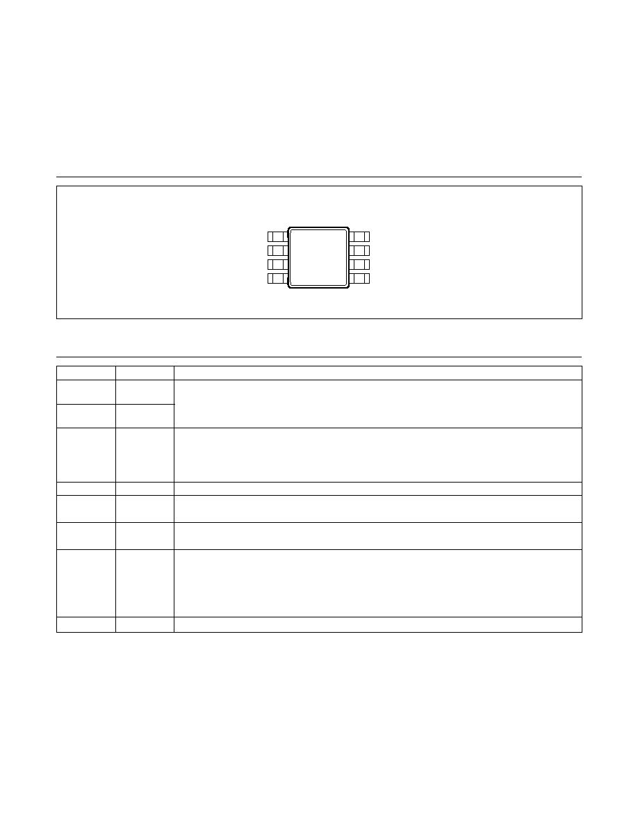
Pin Configuration
Pin Description
PIN
NAME
FUNCTION
1
X1
32.768kHz Crystal Connections. The internal oscillator circuitry is designed for use with a crystal
having a specified load capacitance (CL) of 6pF.
Note: For more information about crystal selection and crystal layout considerations, refer to
Application Note 58: Crystal Considerations with Maxim Real-Time Clocks (RTCs).
2
X2
3
VBAT
Battery Supply Input for Lithium Cell or Other Energy Source. Battery voltage must be held between
the minimum and maximum limits for proper operation. Diodes placed in series between the backup
source and the VBAT pin can prevent proper operation. If a backup supply is not required, VBAT
must be grounded. UL recognized to ensure against reverse charging when used with a lithium cell.
4
GND
Ground
5
SDA
Serial Data Input/Output for the I2C serial interface. It is an open-drain output and requires an
external pullup resistor. The pullup voltage can be up to 5.5V, regardless of the voltage on VCC.
6
SCL
Serial Clock Input for the I2C serial interface. Used to synchronize data movement on the serial
interface. The pullup voltage can be up to 5.5V, regardless of the voltage on VCC.
7
SQW/CLKIN
Square-Wave Output/Clock Input. This I/O pin is used to output one of four square-wave
frequencies (1Hz, 4kHz, 8kHz, 32kHz) or accept an external clock input to drive the RTC counter.
In the output mode (ECLK = 0), it is open drain and requires an external pullup resistor. The
square-wave operates on VCC, or on VBAT with BBCLK = 1. The pullup voltage can be up to 5.5V,
regardless of the voltage on VCC. If not used, this pin may be left unconnected.
8
VCC
Primary Power Supply. Decouple the power supply with a 0.1FF capacitor to ground.
SOP
27
SQW/CLKIN
X2
18
VCC
X1
SCL
VBAT
36
SDA
GND
45
DS1308
TOP VIEW
+
发布紧急采购,3分钟左右您将得到回复。
相关PDF资料
DS1315EN-5/T&R
IC TIME CHIP PHANTOM 20-TSSOP
DS1318E+
IC COUNTER ELAPSED TIME 24-TSSOP
DS1337S+C01
IC RTC SERIAL 2WIRE LP 8-SOIC
DS1338C-33#T&R
IC RTC 56BYTE NV SRAM 16SOIC
DS1339AU+
IC RTC I2C W/ALARM 8USOP
DS1339C-2#
IC RTC I2C W/ALARM 16-SOIC
DS1340Z-33/T&R
IC RTC I2C W/CHARGER 3.3V 8-SOIC
DS1340Z-3
IC RTC I2C W/CHARGER 3V 8-SOIC
相关代理商/技术参数
DS1308U-3+T
功能描述:实时时钟 LOW CUR 3V I2C RTC
RoHS:否 制造商:Microchip Technology 功能:Clock, Calendar. Alarm RTC 总线接口:I2C 日期格式:DW:DM:M:Y 时间格式:HH:MM:SS RTC 存储容量:64 B 电源电压-最大:5.5 V 电源电压-最小:1.8 V 最大工作温度:+ 85 C 最小工作温度: 安装风格:Through Hole 封装 / 箱体:PDIP-8 封装:Tube
DS1308U-33
制造商:MAXIM 制造商全称:Maxim Integrated Products 功能描述:Low-Current I2C RTC with 56-Byte NV RAM
DS1308U-33+
功能描述:实时时钟 LOW CUR 3.3V I2C RTC
RoHS:否 制造商:Microchip Technology 功能:Clock, Calendar. Alarm RTC 总线接口:I2C 日期格式:DW:DM:M:Y 时间格式:HH:MM:SS RTC 存储容量:64 B 电源电压-最大:5.5 V 电源电压-最小:1.8 V 最大工作温度:+ 85 C 最小工作温度: 安装风格:Through Hole 封装 / 箱体:PDIP-8 封装:Tube
DS1308U-33+T
功能描述:实时时钟 LOW CUR 3.3V I2C RTC
RoHS:否 制造商:Microchip Technology 功能:Clock, Calendar. Alarm RTC 总线接口:I2C 日期格式:DW:DM:M:Y 时间格式:HH:MM:SS RTC 存储容量:64 B 电源电压-最大:5.5 V 电源电压-最小:1.8 V 最大工作温度:+ 85 C 最小工作温度: 安装风格:Through Hole 封装 / 箱体:PDIP-8 封装:Tube
DS1310
制造商:未知厂家 制造商全称:未知厂家 功能描述:
DS13-1000
功能描述:固态继电器-PCB安装 HIGH FREQUENCY RELAY
RoHS:否 制造商:Omron Electronics 控制电压范围: 负载电压额定值:40 V 负载电流额定值:120 mA 触点形式:1 Form A (SPST-NO) 输出设备:MOSFET 封装 / 箱体:USOP-4 安装风格:SMD/SMT
DS13-1000S
制造商:TE Connectivity 功能描述:High Performance Solid State Relays
DS13-1001
制造商:MA-COM 制造商全称:M/A-COM Technology Solutions, Inc. 功能描述:DS13 Series High Performance Solid State Relays For Loads Up To 2A@60Vdc